


Four diodes and two paths through a bridge rectifier
The board arranges four diodes in a diamond so both conducting paths can be followed. Light-coloured bands identify the cathodes; the two AC terminals and signed DC terminals sit outside the bridge.
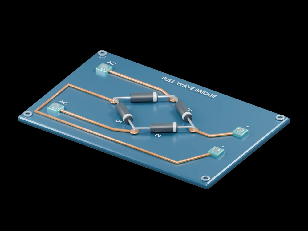
Inside the assembly
Each diode spans two shared copper junctions. Two cathodes meet at the positive output, while two anodes meet at the negative output. Separate copper routes take the AC inputs to the remaining junctions. No smoothing capacitor or load is installed in this demonstration.
Scientific explanation
On each AC half-cycle, a different pair of diodes conducts so current through a connected load keeps the same direction. For ideal diodes, the output follows the absolute value of the input. Real conduction includes two forward voltage drops. Without smoothing, the result is pulsating DC rather than a constant supply.
- vᵢ(t)
- Instantaneous voltage between AC terminals
- vₒ(t)
- Instantaneous positive-to-negative output voltage
Ideal diodes with a resistive load. Reverse recovery, junction heating, leakage and smoothing are omitted; the board is not an energised circuit.
Explore the model
- Find the cathode band on each diode.
- Trace the path from the upper AC junction to positive, then from negative to the lower AC junction.
- Reverse the AC polarity and identify the other pair.
From geometry to engineering
A practical power supply needs diode voltage/current ratings, thermal design, a load and any required filter or regulator. Copper geometry here is illustrative, not a fabrication layout.