


Switching energy through a buck converter
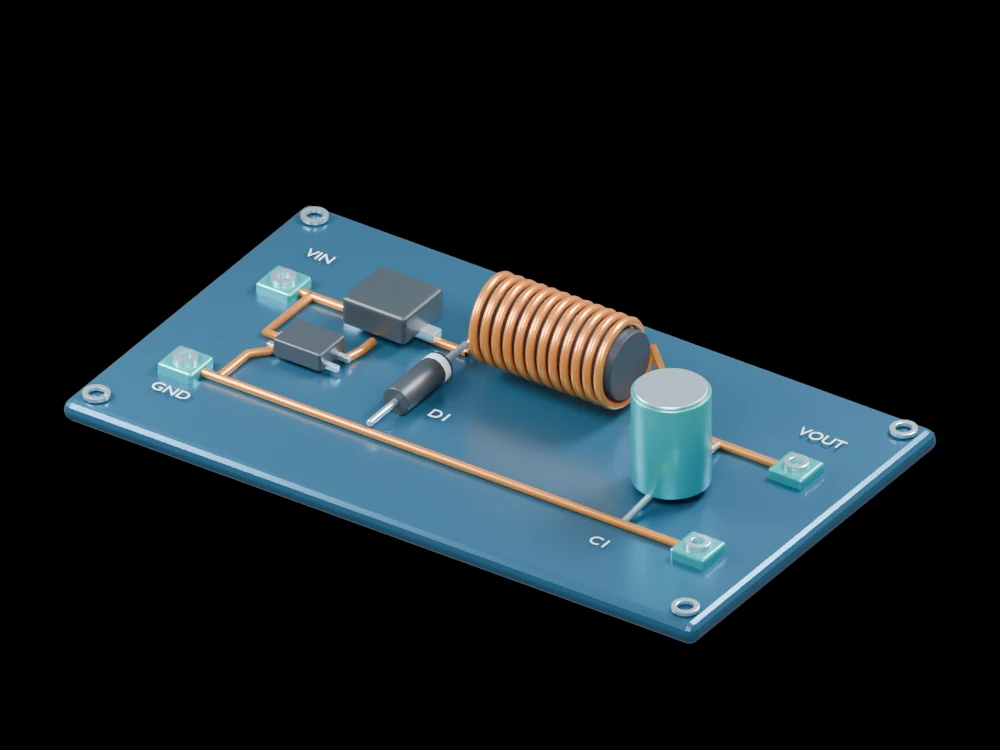
A compact board places the main power-stage components in a visible sequence. Follow the input through the switch and inductor, then inspect the capacitor and return path.
Inside the assembly
The dark Q1 package represents the switching MOSFET. An exposed copper winding surrounds the L1 core; the D1 cathode faces the switch node. A teal output capacitor connects the output rail to the shared return. A small controller package indicates the gate-drive function; its control internals are omitted.
Scientific explanation
A buck converter lowers DC voltage by switching the input to an inductor. During the off interval, the freewheel diode provides a path for inductor current. The inductor and capacitor smooth the switching waveform. In ideal steady continuous conduction, volt-second balance gives an output voltage proportional to the switch duty ratio.
- Vᵢ, Vₒ
- Input and average output DC voltages (V)
- D
- Duty ratio between zero and one
- tₒₙ, T
- Switch on-time and switching period (s)
Ideal components, steady continuous inductor current and negligible ripple for the voltage ratio. This is a power-stage illustration, not a working controller or rated PCB.
Explore the model
- Follow the positive input route into Q1.
- Locate the freewheel diode between return and switch node.
- Trace the output capacitor connections to the output rail and ground return.
From geometry to engineering
A complete design must select switching frequency, inductance, capacitance and device ratings, then verify control stability, losses, current limits and electromagnetic compatibility.