


Two complementary switches: understanding a CMOS inverter
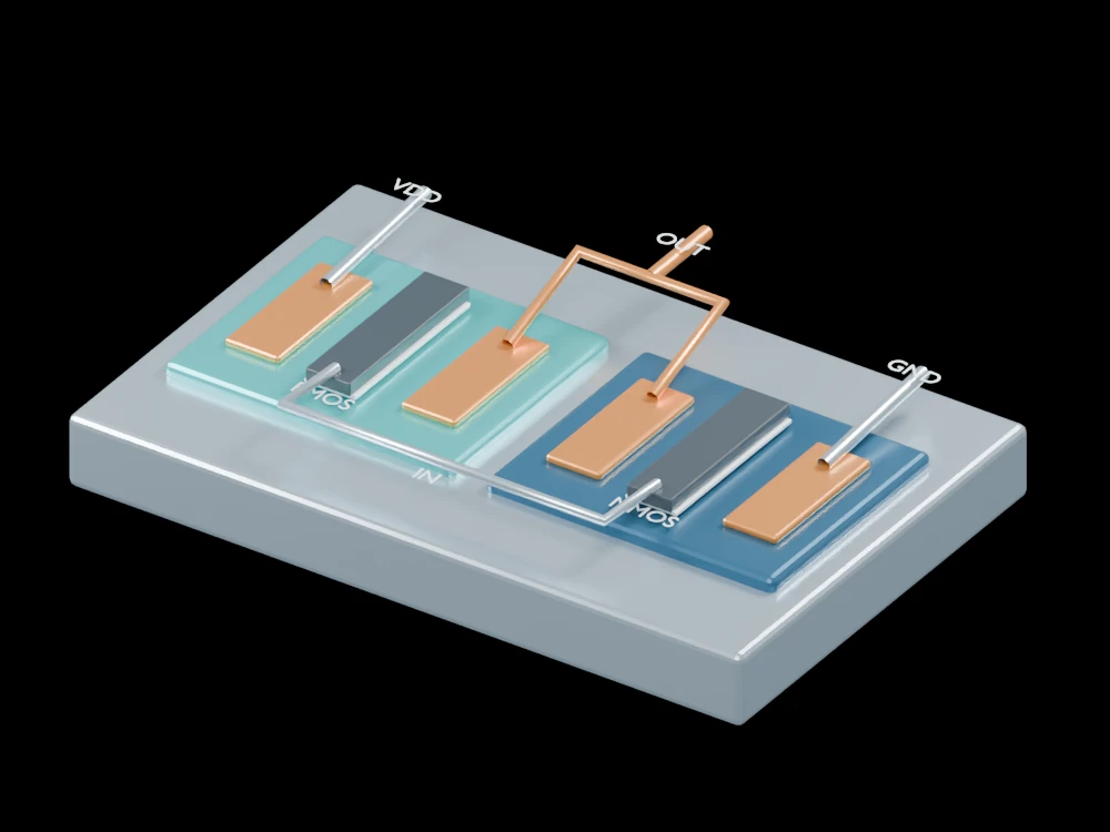
This enlarged layout separates two transistor regions, their gates and the interconnects of a NOT gate. The model makes circuit relationships visible without attempting a fabrication-scale cross-section.
Inside the assembly
Two gates bridge pairs of source and drain regions on the substrate. Metal paths join the gates to one input and the drain regions to one output. Separate rails represent supply and ground. Device layers, contacts and vertical spacing are exaggerated so the connections can be inspected.
Scientific explanation
For valid steady logic levels, a low input turns on the p-channel path to the supply and turns off the n-channel path. A high input reverses those states, pulling the output towards ground. The output is therefore the logical complement of the input.
- A
- Input logic state
- Y
- Output logic state
- VDD, GND
- Positive supply and reference rails
Ideal steady logic operation. Switching transitions, leakage, thresholds and output loading require device models and are not simulated here.
References
Toshiba · Basics of CMOS Logic ICsExplore the model
- Identify the shared input connection between the two gates.
- Trace both drain regions towards the common output.
- Distinguish the supply connection from the ground return.
From geometry to engineering
Use a transistor circuit model to examine the voltage-transfer curve, noise margins and propagation delay before relating a layout to a fabrication process.