


From silicon to pins: inside an integrated-circuit package
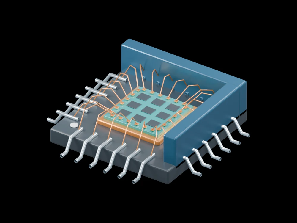
A chip package connects a very small die to a much larger circuit board. Removing two walls exposes the die, bond wires and lead frame in this conceptual assembly.
Inside the assembly
The central silicon block carries a grid of illustrative functional regions. Fine copper loops connect its perimeter pads to the surrounding leads. Twenty-four formed terminals extend beyond the blue package body, and a corner mark identifies the package orientation. The die pattern illustrates organisation rather than a real processor layout.
Scientific explanation
Wire bonds provide electrical paths from die pads to package leads. Even a short conductor has resistance, which depends on its length, cross-sectional area and material. At high frequencies its inductance and surrounding capacitance also matter; a resistance-only model is incomplete.
- R
- Conductor resistance (Ω)
- ρ
- Electrical resistivity (Ω·m)
- ℓ, A
- Conductor length (m) and cross-sectional area (m²)
Uniform conductor and temperature for the resistance expression. Wires and internal features are enlarged for visibility; no package pinout or current rating is specified.
References
Texas Instruments · Assembly and testExplore the model
- Follow one wire from the die pad to its external terminal.
- Compare the raised wire loops with the flat die surface.
- Find the orientation mark and count the six leads on each side.
From geometry to engineering
A package study would specify the die pad map, interconnect material, thermal path and manufacturing clearances, then analyse mechanical and electrical reliability.