

Electronics research · Research insights
Circuits stacked below 300°C offer a route to denser chips
A 2026 demonstration builds complementary logic and memory in vertical layers. Explore the distinction between chip packaging and monolithic 3D circuits.
The package around a silicon die solves one kind of integration problem: connecting and protecting a very small circuit. Inside the die, engineers face another problem. Adding more devices in the same footprint becomes difficult when each new processing step can damage layers already underneath it.
Latest breakthrough
A July 2026 Nature Communications paper demonstrates monolithic three-dimensional complementary circuits using n-type indium oxide and p-type tellurium. The researchers show that the order of the semiconductor layers can be reversed while keeping fabrication below 300°C. Demonstrations include inverters, multilayer logic and a functioning three-dimensional SRAM cell. Here, 'reversible stacking' refers to freedom in the vertical ordering of device types, not to a finished chip being repeatedly peeled apart and reassembled. The result addresses a thermal constraint that limits how circuits can be built above existing circuitry.
Weng and colleagues. Nature Communications (2026). Read the original study.
How the method works
The researchers fabricate complementary devices with n-type indium oxide and p-type tellurium in different vertical orders while keeping processing below 300°C. Complementary circuits use device types with different carrier behaviour, so integration must preserve the functioning of both layers. Inverters, multilayer logic and an SRAM cell then test whether the arrangement supports actual circuit functions. The thermal constraint is central because later processing can damage earlier structures. Demonstrating circuits establishes more than a proposed stack drawing, but remains distinct from a qualified, mass-produced chip process.
A simple analogy
Adding another floor to a finished building is easier if the new work does not damage what is already underneath. Low-temperature processing addresses a comparable integration problem. Semiconductor layers are not structural floors, and their interfaces, electrical connections and defects impose different constraints. The analogy explains why fabrication order and heat exposure matter.
Why the process temperature matters
A completed transistor contains interfaces and materials chosen for particular electrical properties. A later high-temperature process can change those properties. Building upward therefore requires a sequence in which each new layer is compatible with everything below it. The engineering challenge includes both a working individual transistor and the connections that make several layers behave as a circuit.
Density is only one possible benefit
Shorter connections between logic and memory could eventually reduce the effort of moving data around a chip. Our interpretation is that the demonstrated freedom in stacking order may also give designers more ways to arrange a system. Practical value will depend on yield, heat removal and reliability, not simply the number of layers visible in a cross-section.
A working cell is an early milestone
An SRAM-cell demonstration is meaningful evidence that devices can cooperate, but it does not establish a manufacturable high-capacity memory product. Large arrays introduce variation and defect problems that small circuits may not expose. The material choices also differ from conventional silicon CMOS. Scaling and endurance studies are needed before translating the demonstration into a commercial performance claim. The quality of an individual switching device remains important, as illustrated by the new dielectric interface for 2D inverters.
Start with the package, then look inward
The gallery IC package exposes the die, bond pads, bond wires and lead frame beneath a cutaway moulding. Follow how signals reach the die from the external pins. This shows the outer connection problem; the paper investigates structures at a much smaller scale within integrated circuitry. The model does not contain the research transistor stack or its fabrication details.
Related articles
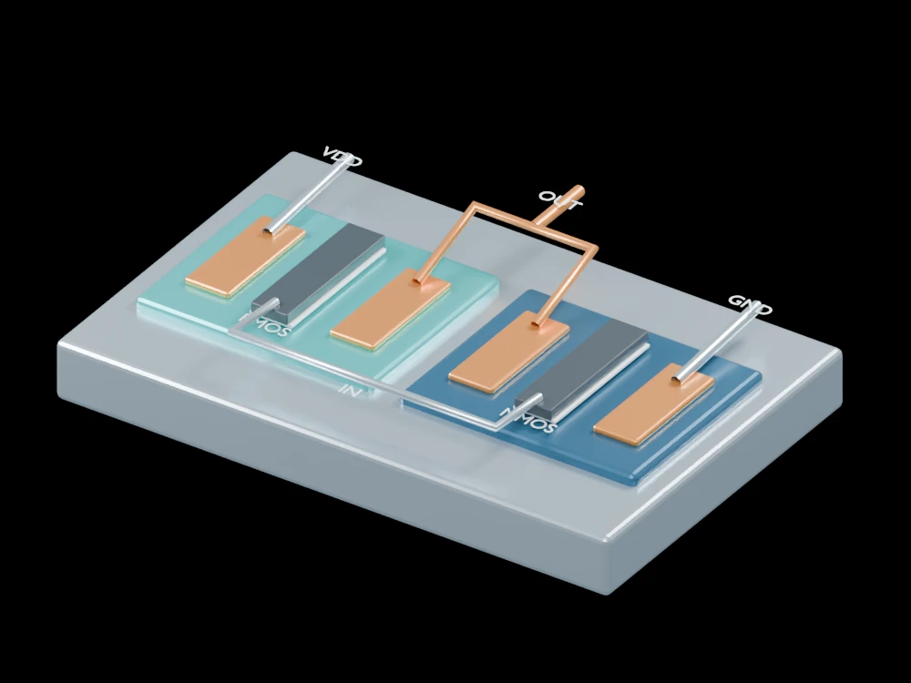 A new gate interface enables 2D inverters with subpicowatt static power
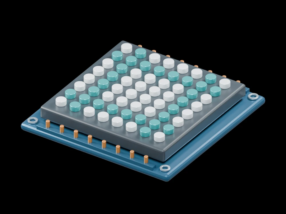 A red micro-LED prototype packs 1,700 pixels into each inch
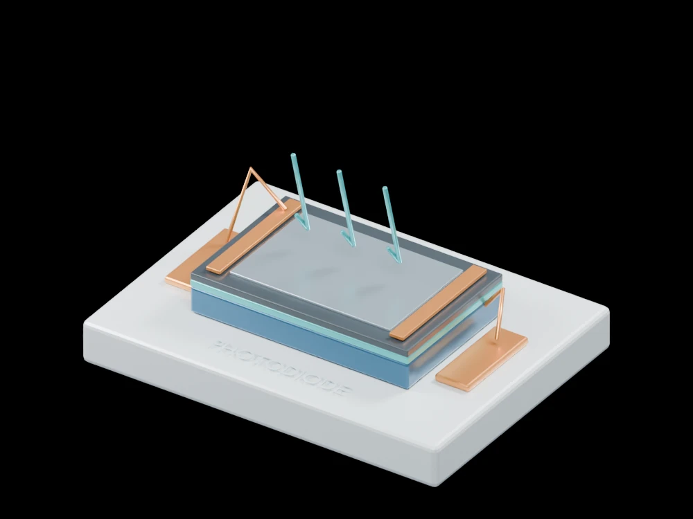 A programmable photodiode brings computation closer to the sensor
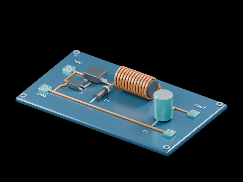 A two-phase buck converter tackles the light-load efficiency problem
 Correcting encoder signals improves tiny-motion measurements
 Better polishing helps quartz vibrations remain coherent for milliseconds
Explore the models
Sources and further reading
- Reversibly Stacked Monolithic 3D Integrated Circuits Published 9 Jul 2026