

Electronics research · Research insights
A red micro-LED prototype packs 1,700 pixels into each inch
Researchers integrated red micro-LEDs with silicon drivers at high pixel density. Explore why shrinking a red emitter changes the design problem.
An LED matrix makes a picture by controlling individual light emitters. Shrinking that arrangement towards a near-eye display introduces difficulties that a large demonstration board does not reveal. A smaller pixel needs suitable light output, efficient current use and a reliable connection to its driver.
Latest breakthrough
A January 2026 Nature Electronics paper reports a red active-matrix micro-LED display with a pixel density of 1,700 pixels per inch. It integrates AlInP/GaInP light-emitting layers with silicon CMOS driving circuits. The work addresses the loss of efficiency that can accompany shrinking red emitters through a particular quantum-well design and monolithic integration approach. This is a fabricated display demonstration. It does not by itself establish a complete full-colour headset, and pixel density should not be confused with brightness, optical resolution or the comfort of a finished near-eye system.
Park and colleagues. Nature Electronics (2026). Read the original study.
How the method works
The demonstration integrates red light-emitting semiconductor layers with silicon CMOS circuitry that drives an active matrix. An active matrix controls pixels individually through associated electronics. The quantum-well design addresses how carrier confinement and emission behave as red emitters become small. Pixel density counts how tightly pixels are placed; it is not a direct measure of how much light reaches the eye through a finished optical system. The fabricated red display tests one important integration problem while leaving the additional requirements of a full-colour product separate.
A simple analogy
Packing more tiny lamps onto a board is useful only if each remains bright enough and can be controlled properly. That captures the linked emitter-and-driver problem. Semiconductor emitters involve carrier physics absent from ordinary lamps, and an eventual headset adds optics and human perception. More pixels alone cannot answer all of those questions.
Small pixels change both optics and electronics
As an emitter shrinks, its surfaces and interfaces become increasingly important relative to its emitting volume. Meanwhile, the circuit must deliver a controlled current to a very small location. A display is consequently a system of emitters and drivers. Improving one while making the other difficult to manufacture may leave the full panel less practical.
Why integration is the central story
Our interpretation is that the significance lies in coordinating emitter design with the underlying electronics. Precise integration could help create compact displays for instruments, viewfinders and wearable systems. To judge those possibilities, an engineer would also need to know uniformity, lifetime, colour performance and manufacturing yield. A dense array is a useful milestone because it brings several of these requirements into one physical object.
What the result leaves open
The paper focuses on red emission and its specific device structure. Combining red, green and blue channels introduces further materials and alignment questions. Operating temperature and the optics placed in front of the display can also change the viewer's experience. The study supplies evidence about an integrated microdisplay, rather than a guarantee that every future display will be more efficient or comfortable. Placing electronics close to their function also motivates research on vertically stacked complementary circuits, although a display has additional optical requirements.
Follow a pixel through the matrix
In the gallery LED matrix, inspect the 64 emitter lenses and the row and column terminals. The separated routing planes make it easier to see how many emitters can be addressed in a regular arrangement. This is a larger-scale teaching model. It illustrates array organisation, while the paper's active-matrix microdisplay uses different dimensions, materials and driver integration.
Related articles
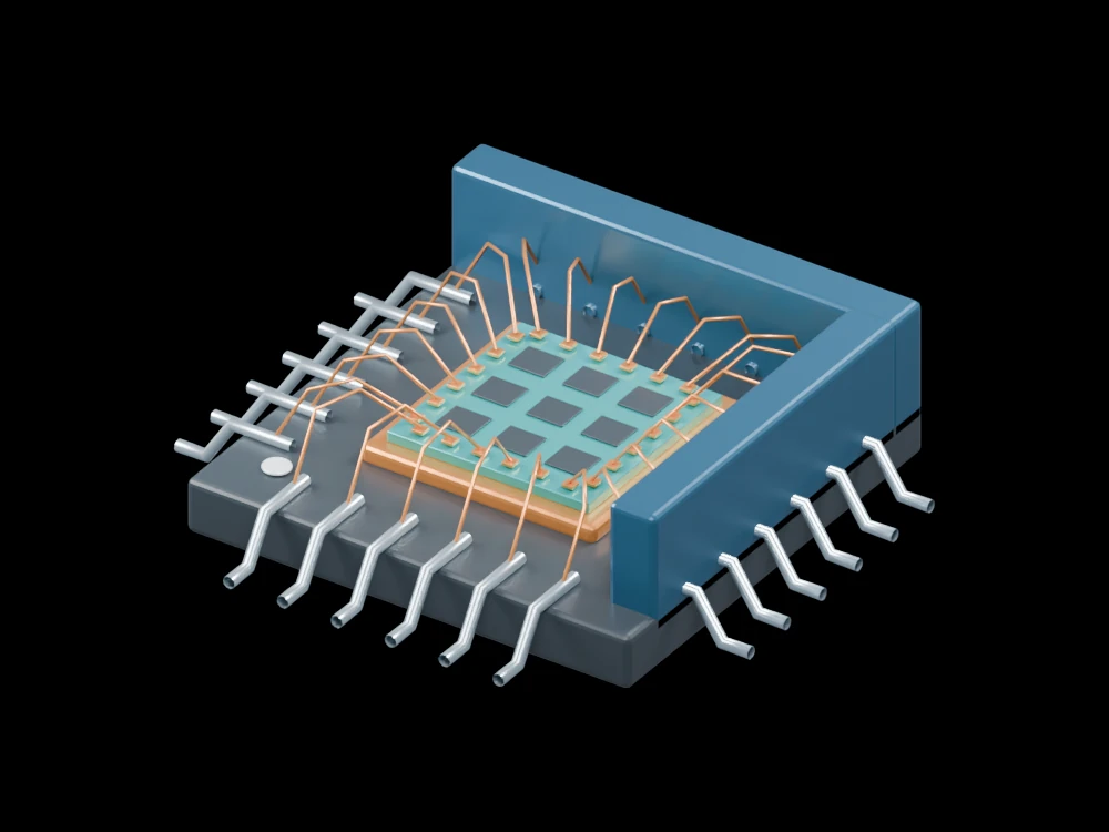 Circuits stacked below 300°C offer a route to denser chips
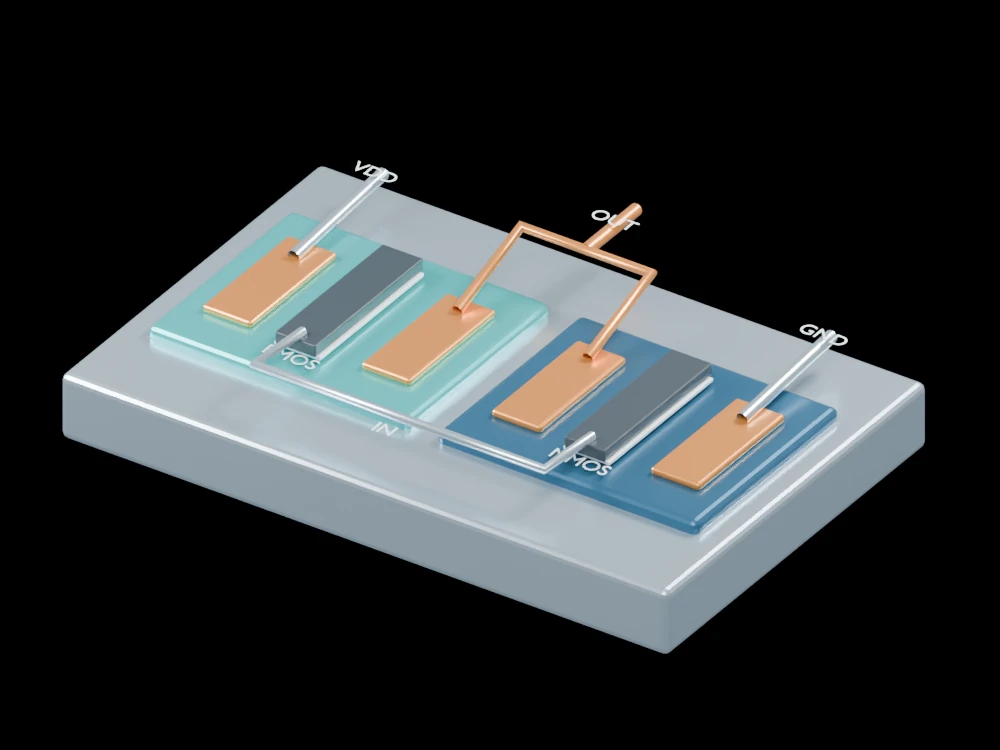 A new gate interface enables 2D inverters with subpicowatt static power
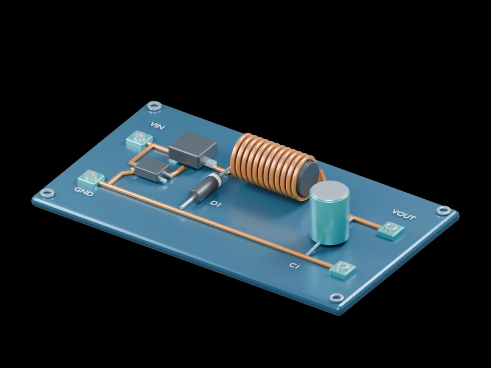 A two-phase buck converter tackles the light-load efficiency problem
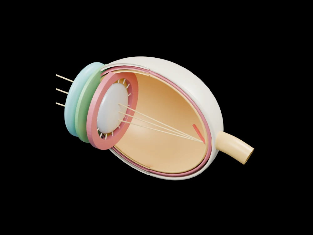 An artificial retina turns near-infrared light into signals in mice
 Correcting encoder signals improves tiny-motion measurements
 A programmable photodiode brings computation closer to the sensor
 Better polishing helps quartz vibrations remain coherent for milliseconds