

Power electronics · Research insights
Complementary GaN logic puts both transistor types on one substrate
A 2021 Nature Electronics study demonstrates complementary GaN logic gates, a foundational step toward more integrated wide-bandgap electronics.
Study published: 19 July 2021 · Nature Electronics. Original research commentary by NPT Research.
Efficient power conversion needs a capable switch and a controller that tells it when to act. Gallium nitride is valuable in power devices, but integrating complementary control logic has been difficult. A foundational study tackled the missing pairing of transistor types on a common substrate.
Latest breakthrough
The researchers integrated enhancement-mode n-channel and p-channel GaN field-effect transistors monolithically. They built NOT, NAND, NOR and transmission gates, and demonstrated latch cells and ring oscillators. The inverters showed rail-to-rail operation, suppressed static power dissipation and thermal stability under the reported tests.
Read the original study: Gallium nitride-based complementary logic integrated circuits.
How the study worked
Fabrication placed both transistor types into a shared GaN technology. Electrical measurements first characterized the individual devices and then the combined logic circuits. Cascading gates into oscillators tested whether the building blocks could work as connected systems rather than only as isolated demonstrations.
The idea in everyday terms
Complementary logic is like a pair of coordinated valves: one provides a route toward one supply level, while the other provides a route toward the opposite level. Good coordination avoids leaving both routes open unnecessarily. The analogy captures static power management, although real transistors also have capacitance and switching losses.
Why it matters
Integrating control and power functions can shorten electrical paths and reduce the need for separate technologies in selected designs. That possibility connects naturally with new GaN power-switch architectures. It is a platform advance that enables further circuit engineering rather than a complete product by itself.
What the evidence does not establish
The paper demonstrates logic building blocks, not a finished buck converter or a universal replacement for silicon CMOS. Logic quality, manufacturing yield, protection functions and power-device compatibility all need attention before integration can deliver practical system benefits.
Explore the device
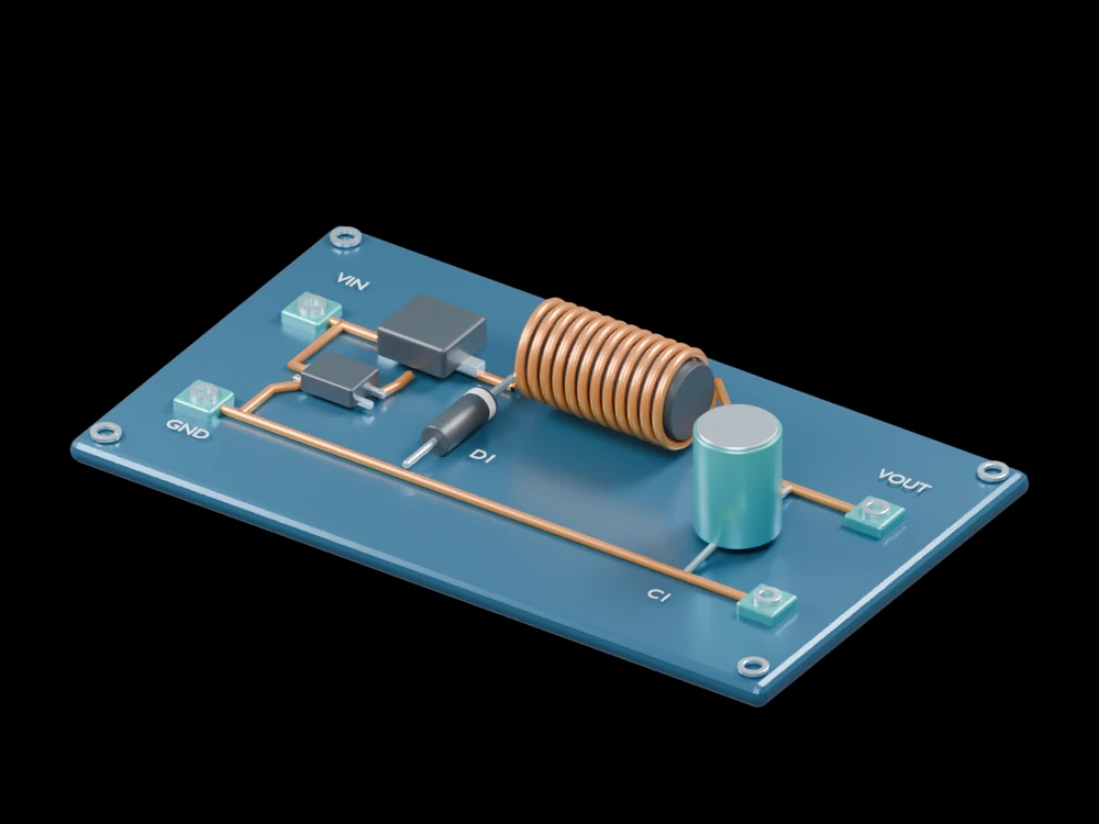
In the buck model, imagine the control circuitry that must operate the visible switch at the right time. This study explains one route to making that control more compatible with GaN devices. Device-level cooling research addresses another constraint that integration alone cannot remove.
Explore the DC buck converter model and its description, or read our earlier device-focused research explanation.
Primary citation: Zheyang Zheng, Li Zhang, Wenjie Song et al.. Gallium nitride-based complementary logic integrated circuits. Nature Electronics (2021). 10.1038/s41928-021-00611-y.
Related articles
 Boron arsenide draws heat from working GaN transistorsBuilt-in crystal polarization helps GaN switches withstand higher voltageA two-phase buck converter tackles the light-load efficiency problemA vibrating resonator helps a DC converter step down voltage efficiently
 Nanoscale spin rectifiers turn weak radio signals into useful powerA superconducting chip brings full-wave rectification into the coldElemental tellurium turns radio signals into a tunable room-temperature outputTin telluride rectifies signals from megahertz to terahertz without external bias
 A 100 kW solid-state transformer reaches 98.57% efficiency in testingA magnetic composite tackles eddy-current and hysteresis losses togetherNarrow magnetic domains help an iron-rich ribbon waste less energyMagnetic-domain motion can send energy into the crystal latticeEngineered interfaces let magnetic particles couple without the usual loss penaltyA quantum material rectifies signals from radio to terahertz bands
 A rotating magnetic field steers crystallisation toward finer soft magnetsAn alloy becomes mechanically strong while remaining magnetically softTiny manufacturing deformations can disturb the magnetic structure of motor steelNanoprecipitates push ductile soft magnets toward two-gigapascal strength
 An electrically heated foam brings heat inside a catalyst bed
 A redesigned magnetic path cuts opening time in a solenoid study
Explore the models
Sources and further reading
- Gallium nitride-based complementary logic integrated circuits Published 19 Jul 2021