

Power electronics · Research insights
Boron arsenide draws heat from working GaN transistors
A Nature Electronics study integrates boron-arsenide cooling substrates with GaN devices and measures the thermal interface, rather than relying on bulk conductivity alone.
Study published: 17 June 2021 · Nature Electronics. Original research commentary by NPT Research.
A material can conduct heat extremely well and still make a disappointing cooler if heat cannot cross the interface into it. Researchers tackled both sides of this problem by integrating boron arsenide with working gallium-nitride devices and examining the boundary between them.
Latest breakthrough
The study reported high thermal boundary conductance in GaN-on-boron-arsenide structures and lower transistor hot-spot temperatures than the compared diamond and silicon-carbide configurations at the same transistor power density. The result demonstrates why the material interface and the complete device must be evaluated together.
Read the original study: Integration of boron arsenide cooling substrates into gallium nitride devices.
How the study worked
The team combined heterogeneous integration, thermal measurements and modelling of energy transport. Working AlGaN/GaN high-electron-mobility transistors provided a device-level test. Calculations of phonon behaviour helped interpret how the substrate and interface move thermal energy away from the heat-generating region.
The idea in everyday terms
A fast motorway is useful only if traffic can reach it through the entrance. Bulk thermal conductivity resembles the motorway; interface conductance resembles that entrance. Improving one while neglecting the other can leave the same bottleneck in place. In the actual device, the travelling excitations are mainly lattice vibrations rather than vehicles.
Why it matters
Power converters repeatedly generate heat in small switching regions. A clearer understanding of substrate integration can inform thermal design, including future implementations of high-voltage GaN switches. Cooling channels built into power chips attack the same system problem through a different route.
What the evidence does not establish
The paper’s transistor demonstrations concern the tested device structures, including radiofrequency applications. They do not directly establish a cooler commercial buck converter or a universal ranking of all diamond packages. Interface preparation, reliability and manufacturing cost are essential to any translation.
Explore the device
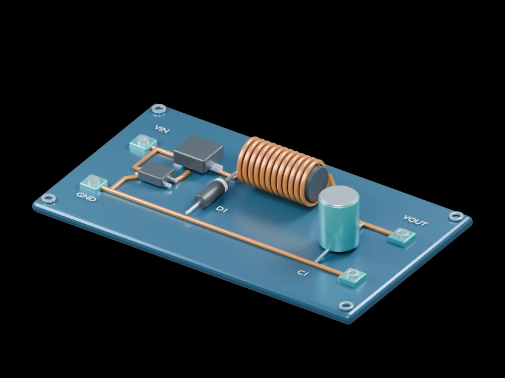
The buck-converter model shows the circuit components, but its geometry does not reveal a transistor’s internal hot spot. This article adds that missing thermal scale. Better cooling supports the electrical design; it does not remove the need to minimise switching and conduction losses in the first place.
Explore the DC buck converter model and its description, or read our earlier device-focused research explanation.
Primary citation: Joon Sang Kang, Man Li, Huan Wu et al.. Integration of boron arsenide cooling substrates into gallium nitride devices. Nature Electronics (2021). 10.1038/s41928-021-00595-9.
Related articles
 Built-in crystal polarization helps GaN switches withstand higher voltageA two-phase buck converter tackles the light-load efficiency problem
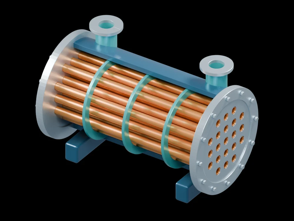 Cooling channels built with the electronics remove heat closer to its sourceComplementary GaN logic puts both transistor types on one substrateA vibrating resonator helps a DC converter step down voltage efficiently
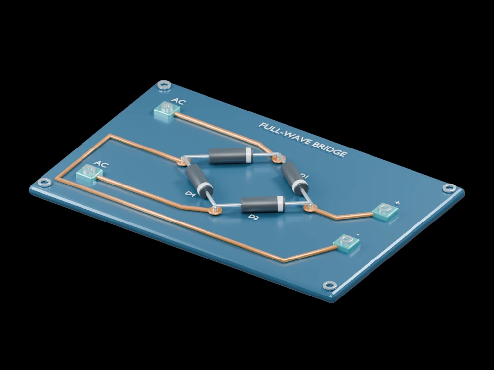 Nanoscale spin rectifiers turn weak radio signals into useful powerA superconducting chip brings full-wave rectification into the coldElemental tellurium turns radio signals into a tunable room-temperature outputTin telluride rectifies signals from megahertz to terahertz without external bias
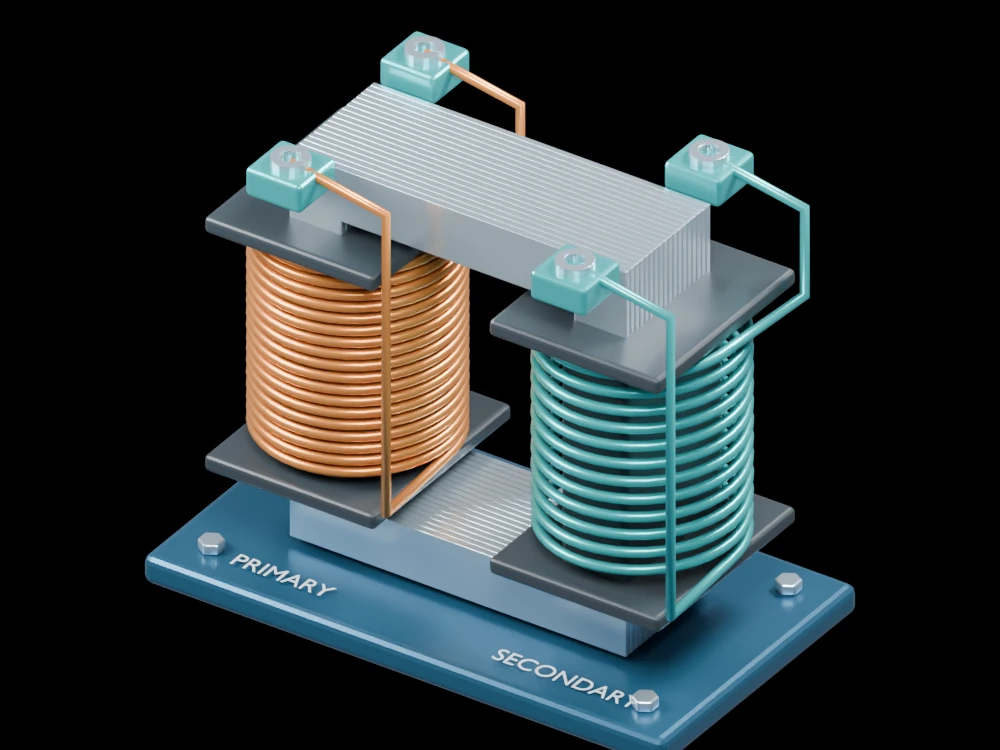 A 100 kW solid-state transformer reaches 98.57% efficiency in testingA magnetic composite tackles eddy-current and hysteresis losses togetherNarrow magnetic domains help an iron-rich ribbon waste less energyMagnetic-domain motion can send energy into the crystal latticeEngineered interfaces let magnetic particles couple without the usual loss penaltyA quantum material rectifies signals from radio to terahertz bands
 A rotating magnetic field steers crystallisation toward finer soft magnetsAn alloy becomes mechanically strong while remaining magnetically softTiny manufacturing deformations can disturb the magnetic structure of motor steelNanoprecipitates push ductile soft magnets toward two-gigapascal strength
 An electrically heated foam brings heat inside a catalyst bed
 A redesigned magnetic path cuts opening time in a solenoid study
Explore the models
Sources and further reading
- Integration of boron arsenide cooling substrates into gallium nitride devices Published 17 Jun 2021