

Power electronics · Research insights
Built-in crystal polarization helps GaN switches withstand higher voltage
A Nature Electronics study uses balanced electron and hole layers to spread electric fields in GaN power devices without intentional superjunction doping.
Study published: 28 August 2026 · Nature Electronics. Original research commentary by NPT Research.
Power switches face a persistent compromise: they should resist voltage when off, yet waste little energy when conducting. Sharp concentrations of electric field make that balance harder. A new GaN device architecture uses the crystal’s own polarization to redistribute the electrical stress.
Latest breakthrough
The researchers formed intrinsically charge-balanced superjunctions using mobile electron and hole layers in III-nitride heterostructures. They reported Schottky diodes exceeding 3.9 kV breakdown and transistors exceeding 3.4 kV. Contacting the hole layer allowed both carrier populations to deplete during switching, helping maintain field balance.
Read the original study: Intrinsic polarization superjunctions in III-nitride heterostructures for efficient power electronics.
How the study worked
The team fabricated GaN-on-silicon devices and measured their voltage-blocking and conducting behaviour. Dynamic measurements checked whether on-resistance worsened after high-voltage operation. These measurements are important because an impressive static breakdown result alone does not establish an efficient switching device.
The idea in everyday terms
The problem resembles distributing a heavy load across a wide support instead of concentrating it at one sharp corner. The superjunction shapes where electrical stress develops. Unlike a physical beam, however, its balance changes as charge carriers move, so switching tests are essential to the explanation.
Why it matters
Better field management can support compact, efficient power electronics if the benefits survive integration into circuits. A buck converter is one useful context for understanding repeated switching. Integrated GaN logic addresses the commands sent to those switches; resonator-based conversion changes how energy is transferred afterward.
What the evidence does not establish
These are device-level results, not a demonstrated efficiency increase for a complete commercial buck converter. Breakdown voltage is also not automatically the safe continuous operating voltage. Packaging, protection, reliability and switching losses remain separate engineering questions.
Explore the device
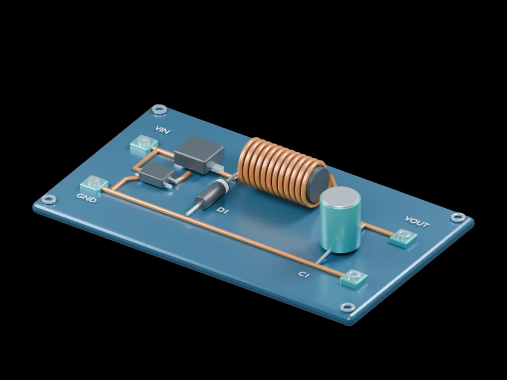
Use the buck-converter model to locate the switching element and its connection to the energy-storage components. The research concerns the internal semiconductor structure of that element, which the model does not resolve. The value is a new device design principle, rather than a new arrangement of visible circuit-board parts.
Explore the DC buck converter model and its description, or read our earlier device-focused research explanation.
Primary citation: Luca Mazzone, Yuan Zong, Hongkeng Zhu et al.. Intrinsic polarization superjunctions in III-nitride heterostructures for efficient power electronics. Nature Electronics (2026). 10.1038/s41928-026-01691-4.
Related articles
 Complementary GaN logic puts both transistor types on one substrateA vibrating resonator helps a DC converter step down voltage efficientlyA two-phase buck converter tackles the light-load efficiency problemBoron arsenide draws heat from working GaN transistors
 Nanoscale spin rectifiers turn weak radio signals into useful powerA superconducting chip brings full-wave rectification into the coldElemental tellurium turns radio signals into a tunable room-temperature outputTin telluride rectifies signals from megahertz to terahertz without external bias
 A 100 kW solid-state transformer reaches 98.57% efficiency in testingA magnetic composite tackles eddy-current and hysteresis losses togetherNarrow magnetic domains help an iron-rich ribbon waste less energyMagnetic-domain motion can send energy into the crystal latticeEngineered interfaces let magnetic particles couple without the usual loss penaltyA quantum material rectifies signals from radio to terahertz bands
 A rotating magnetic field steers crystallisation toward finer soft magnetsAn alloy becomes mechanically strong while remaining magnetically softTiny manufacturing deformations can disturb the magnetic structure of motor steelNanoprecipitates push ductile soft magnets toward two-gigapascal strength
 An electrically heated foam brings heat inside a catalyst bed
 A redesigned magnetic path cuts opening time in a solenoid study